Schematic
One of the purposes of this lab is to design (from netlist to layout) a TSPC (True Single Phase Clock) dynamic flip-flop standard cell. The schematic diagram of this cell is shown in the following figure:
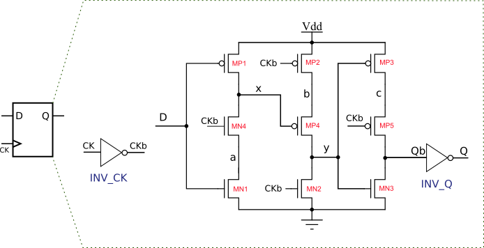
As you may see, the design is based on mos transistors and invertors.
Design of TSPCFF schematic
WARNING : During the design, when creating cells or pins, please stick to the names, and cases (uppercase or lowercase) given in the project.
A. Schematic with Schematics XL
To start the schematic of the DFF_CORE cell use:
CIW -> File -> New -> Cell View
Library |
Cell |
View |
Open with |
TSPCLIB |
TSPCFF |
schematic |
Schematics XL |
We will note SXL the start from the drop-down menus of this schematic editor.
Note
Some commands to begin:
To move an object use SXL -> Edit -> Move
To delete an object use SXL -> Edit -> Delete
Press the escape key`` to exit the last command mode or when you are lost…
B. Pins instantiation
Instantiate and place the input pins in the schematic:
use SXL -> Create -> Pin
Direction |
Pin Names |
Input |
D CK |
Place the pins at the left of the window. Each time you click in the schematic window, you add a new pin of the list.
Instantiate and place the output pin :
Output |
Q |
Place the pin at the right of the window.
Then create the supply pins
Inout |
VDD VSS |
Place the pins at the top left, and top right of the window ( as in the DFF cell)
Exercise with the “move command”, in order to understand the way the editor is working:
Selection of a command (like move)
Click on the object to move
Click on the destination point
Use the escape Key in order to exit the move mode
C. Clock Invertor instanciation
We will use the contents of the INVXL gate from gsclib library. For that purpose we will copy part of the schematic of this cell inside the TSPCFF cell.
- Open the schematic of the INVXL gate from the gsclib library:
From the Library Manager select:
Library |
Category |
Cell |
View |
gsclib045 |
INV |
INVXL |
schematic |
and using the right button -> Open (Readonly)
With the mouse, select all component and wires, excluding the input/output pins
Hit the c key from the keyboard in order to swith to copy mode.
Click (left button) somewhere in the area to copy (starting point of the copy)
Click now (left button) inside the TSPCFF schematic window (destination of the copy)
Hit the escape key in oder to exit the copy mode.
D. Output Invertor instanciation
We will use the contents of the INVX1 gate from gsclib library. For that purpose we will copy part of the schematic of this cell inside the TSPCFF cell. The width of the transistors from this cell are a bit larger in order have a good fanout at the Q output.
- Open the schematic of the INVX1 gate from the gsclib library:
From the Library Manager select:
Library |
Category |
Cell |
View |
gsclib045 |
INV |
INVX1 |
schematic |
and using the right button -> Open (Readonly)
With the mouse, select all component and wires, excluding the input/output pins
Hit the c key from the keyboard in order to swith to copy mode.
Click (left button) somewhere in the area to copy (starting point of the copy)
Click now (left button) inside the TSPCFF schematic window (destination of the copy)
Hit the escape key in oder to exit the copy mode.
E. Transistors instantiation
We will choose standard NMOS and PMOS transistors from the GPDK045 technology. The choosen geometries for the transistors will be as follows:
All transistors will have the standard minimum length in that technology:
45nmNMOS transistors will have a
145nmwidth.PMOS transistors will have a
215nmwidth.
Instantiate the NMOS transistors: use SXL ->
Create->Instance, then choose
Library |
Cell |
View |
Names |
gpdk045 |
nmos1v |
symbol |
MN1 MN2 MN3 MN4 |
Change: Finger Width -> 145n and place (click in schematic window) all NMOS in agreement with the TSPCFF_CORE schematic
Instantiate the PMOS transistors: use SXL ->
Create->Instance, then choose
Library |
Cell |
View |
Names |
Finger Width |
gpdk045 |
pmos1v |
symbol |
MP1 MP2 MP3 MP4 MP5 |
Change: Finger Width -> 215n and place (click in schematic window) all PMOS in agreement with the TSPCFF_CORE schematic
F. Adding Wires
It’s now time to add some wires to the schematic.
use SXL -> Create -> Wire
Click, and then move the pointer to the second point and click to draw the wire. A
double clickends the wire.Don’t forget to connect the bulk of the NMOS (resp PMOS) transistors to the ground (VSS) resp. to the power supply (VDD).
G. Adding Wires Names
All unamed wires should be named, in order to ease the layout phase.
Wires connected to a pin are already named.
To add a label the wire use: SXL -> Create -> Wire Name
Names: x y a b c CKb Qb
Then place the cursor over a wire and click. The name should switch to the next one on the list.
Note
To reduce the amount of wires necessary for the clock (CKb) you can draw a isolated short wire and give it a name “CKb”.
Copy (SXL -> Edit -> Copy) this short wire and connect it to clock pins (input pin and mos gates).
Simulation of the TSPCFF schematic
To validate the schematic level description we will perform a simulation of the cell.
From virtuoso using the Analog Design Environment (ADE)
Simulation with ADE
From the schematic view of the cell use Launch, ADE L
We will note ADE the start from the drop-down menus of the analog design environment.
select ADE ->
setup->Simulator/Directory/Hostand changeProject Directoryto./ADEselect ADE ->
setup->StimuliSetup VDD and VSS
Source |
Function |
Type |
DC Voltage |
VDD |
dc |
Voltage |
1.1 |
VSS |
dc |
Voltage |
0 |
Setup inputs D and CK waveforms.
Input |
Function |
Type |
Voltage 1 |
Voltage 2 |
Period |
D |
Pulse |
Voltage |
0 |
1.1 |
7n |
CK |
Pulse |
Voltage |
0 |
1.1 |
3n |
Setup the simulation time: ADE ->
Analysis->Choose->tran(Stop Time = 25n,Enabled)Setup the signals you want to examine : ADE ->
Outputs->To Be Plotted->Select On Schematicand select CK, D and QThen launch the simulation : ADE ->
Simulation->Netlist and RunCheck that your DFF has a good behavior.
Examine also the internal signals (a, b, c, x, y) during the simulation. Try to explain the obtained waveforms (your explanations should be written your your report).