Layout
TSPCFF layout
Automatic generation of a Virtuoso schematic
Inside you last simulation directory of the TSPCFF cell, launch the following command:
make import_cell
You should now have a new directory named TSPCFF_lib in the main directory of your project.
Launch Virtuoso tool in the main directory of your project:
/comelec/soft/bin/virtuoso
In the library browser you should find a new library named TSPCFF_lib and containing a schematic view of your cell.
Setting up Layout XL
From the schematic view of the cell use
Launchand thenLayout XL.Click OK for default
Startup Optionsand OK again to create new file (Library:<your library>, Cell:<your cell>, View: layout). The schematic window and the layout window are opened side by side.An other window, the layer selection window (LSW) is associated to the layout. From this, you can select (left mouse click) a mask level or set its visibility (middle button) or selectivity (right button).
The top part of layout window contains a set of drop-down menus. We will note LXL the start from this menu.
The goal now is to complete the layout in line with that of schematic.
Before starting the actual layout editing, we will set some optional parameters in Layout XL.
Use LXL ->
Options->Displayto set the following parameters:
Display Controls->Display Levels: set Stop to 20
Grid Controls: setX Snap and Y Snap spacingto 0.005 (This must be conform to the default grid specified in the design rules manual)
We are now ready to start the layout editing. To do that, use:
LXL ->
Connectivity->Generate->All From Source
The Generate Layout form is displayed.
Check the box
Chainingin generate tab (explained below)Select the default
Metal1layer for I/O pins and click OK.
This generate all the transistors, I/O pin in the layout view.
WARNING Do not suppress the Metal1 I/O pins from the layout.
Chained devices
The chaining combine drain and source in order to save layout space:
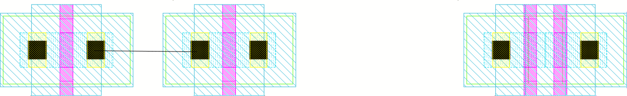
Chained devices are normally in place from the layout generation phase but you can move transistors independantly at any time.
** WARNING** The automatic chaining of transistors may lead to complicated topologies. Take time to examine chaining, and try eventually to update chaining to more suitable topologies
Cell template
The gsclib045 standard cells use a common grid factors that is defined in a programmable cell named cellTmpl as following :
Standard Height = 1.71u (Ref: The boundary box height - middle of VSS rail to middle of VDD rail)
Parametrizable Width
All needed masks for PWELL and NWELL areas as well as body-ties are allready included in the cell.
To facilitate the layout phase, we will instantiate this template cell in the layout.
use LXL -> Create -> Instance
Library Name -> gsclib045_tech, Cell Name -> cellTmpl, View Name -> layout
Place the cell at the (0,0) coordinates of the view. For that purpose:
Edit the properties of the cell (press key “q” on the selected cell). Then fill the values for
Origin: XandY.
Modify the width of the cell in order to be sure that all transistors may be contained inside the cell. As a starting point you may use a width of 3um. For that purpose:
Edit the properties of the cell, select the
parametertab and changee theCell Widthto3
Layout assistants
All components and connexions may be cross viewed in the layout and schematic view. To be able to show incomplete connexions, use:
LXL -> Windows -> Assistants -> Annotation Browser
You can highlight some or all incomplete connexions from this Annotation Browser.
This can be usefull in the device placement to minimize connections. You can use this to place all MOS devices properly (PMOS on Pimp layer, NMOS on Nimp layer)
Design rules verification
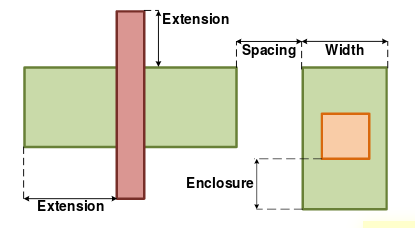
The objective associated with layout rules is to obtain a circuit with the best compromise between yield and performance in the smallest possible area.
The most basic design rules are shown in the following figure:
Design rule verification is made with the Assura tool from Cadence.
First, check the technology for Assura tool: LXL -> Assura -> Technology
Verify that the name of the assura library is:
/comelec/softs/opt/opus_kits/CADENCE_PDKS/gpdk045_v_4_0/assura_tech.lib
We can run the Design Rule Checker with LXL -> Assura -> run DRC
Give a Run Name, a Run Directory and select the gpdk045 technology.
After the verification process, the Error Layer Window shows the rules violations. At this level of the design, you normally have many errors related to minimum area for Metal1 and Poly, Nwell connection… Do not worry, we will address this after proper placement and connection drawing. Check the design rules manual (GPDK045-DRC) for more information.
Connections drawing
Choose the appropriate layer from LSW and then LXL -> Create -> Wiring -> Wire
For Via use LXL -> Create Via
When all incomplete Nets are resolved, check for DRC until you have no error.
Layout versus schematic
Now that we have a complete layout view with design rules conformity, we have to verify the correspondance between the electrical graph of the schematic and the one extracted from the layout. We will also use the Assura tool from Cadence to this end :
LXL -> Assura -> run LVS
In the configuration window run Assura LVS, set a run Name, a run Directory. Then select the gpdk045 technology click OK and wait for the end of the comparaison process. After the run, the tool will report if the schematic and the layout matches. There is also an option to open the LVS Debug view, to look for possible errors in the design matching. If you have any errors, correct them and re-run the LVS.
Parasitic extraction
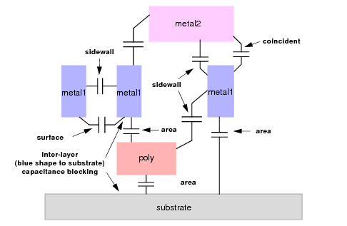
Parasitic extraction is the process by which layout geometries are analyzed and converted to equivalent circuit values for simulation and verification of electrical performance.
For example, the following figure illustrates a cross-sectional view of different intralayer and inter-layer parasitic capacitance components.
We will use the QRC tool from Cadence to perform this task. It will be run also from the Assura menu of Layout XL:
LXL -> Assura -> run Quantus QRC
Fill the QRC Parasitic Extraction Run Form with the appropriate values :
Setup:
Output -> spice, Name -> TSPCFF.sp
Check the box: Extract MOS Diffusion Res
Extraction:
Extraction Type -> RC, Cap Coupling Mode -> Coupled, Ref Node -> VSS
Netlisting
Parasitic Capacitor and Resistor Models -> Do Not Include
Let the other tabs to their default configuration and click OK.
At the end of the process, you have the extracted netlist in the file TSPCFF.spi.
Edit this file to see the parasitic resistors and capacitors extracted by QRC
Contents of your report
The final report should contain
A view of the layout of our gate.
The area of the gate
Some explanations on the topology choices made
Your opinion about the quality of your design.