TSPCFF netlist and environment preparation
One of the purposes of this lab is to design (from netlist to layout) a TSPC (True Single Phase Clock) dynamic flip-flop standard cell.
Directory setup
Prepare a new template directory based on the previous simulation (INV_cell_rise).
Rename the template directory to (TSPCFF_cell_rise)
Inside the directory, rename the INV.vams netlist to TSPCFF.vams.
Modify the
Makefilefile in order to give the name of you DFF netlist (line DUT_FILE=… at the beginning of the code)
TSPCFF netlist
The schematic diagram of this cell is shown in the following figure:
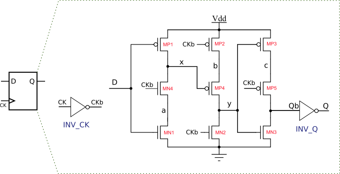
We now want to modify the contents of TSPCFF.vams in order to code a Verilog-AMS netlist of the TSPCFF module.
In the same way as the INV module already defined, add a new TSPCFF module in the file:
With the correct name (TSPCFF)
With the correct list of input and outputs signals (CK, D, Q, VDD, VSS)
All this signals should be defined as inout signals
All this signals should be defined as electrical signals
Each internal node (x, b, c…) should declared and defined as electrical signals
NMOS (resp PMOS) transistors are instanciations of a g45n1svt (resp g45p1svt) module.
NMOS transistors should have a 145e-9 meter width.
PMOS transistors should have a 214e-9 meter width.
You may directly instanciate invertors inside your cell. For that purpose just add a lines of the form:
INV XXX(.A(...), .Y(...), .VDD(...), .VSS(...));`
where:
XXX is the name given to the instance
… are names of signals connected to the I/O of the invertors.
Invertor parametrization
As we eventually want to compare the TSPCFF flipflop with the DFFQX1 flipflop from the gsclib045 library, we want to use the same size of transistors for the CK input invertor, and for the Q output invertor as in the DFFQX1.
Check the the size of transistors for this two invertors in the DFFQX1 gate.
We will now modify the INV gate in order to introduce parameters.
In the INV module, add the two following lines, just after the definitions of the I/Os:
parameter WN=145e-9 ;
parameter WP=214e-9 ;
Then modify the transistors instanciation using the WN and WP parameters instead of the constants values.
You may now choose to modify the default values of WN and WP when instanciating the invertors into the TSPCFF module. For that purpose rewrite the instancisation as follows:
INV #(.WN(YYY), .WP(ZZZ)) XXX(.A(...), .Y(...), .VDD(...), .VSS(...));`
where YYY and ZZZ are the desired constant values.
We will now prepare the simulation itself