Quartus - Getting Started
2022-2026
This is a short guide to start a design on a DE1-SoC board.
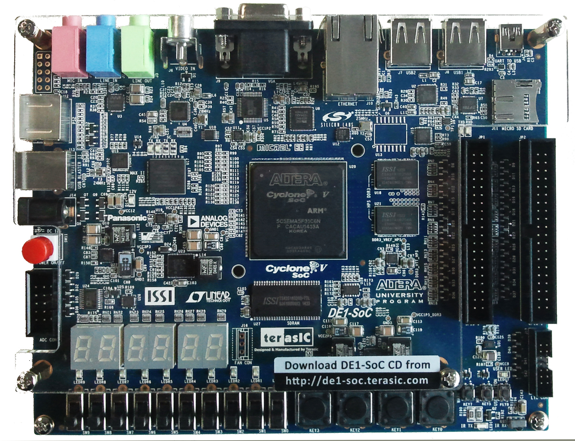
The DE1-SoC Board is an FPGA board designed by Terasic and Altera/Intel for teaching and student projects.
The complete User Manual can be downloaded HERE
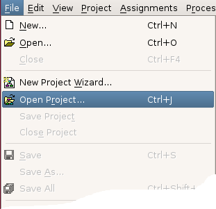
tar xzvf de1-soc.tar.gzquartus &From Quartus GUI, select Open Project from the File menu
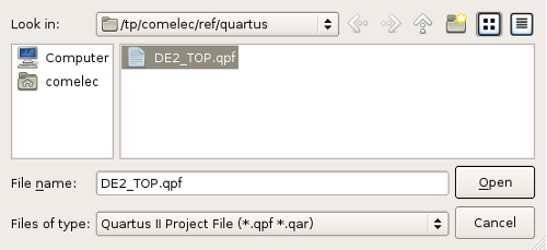
Then selected the project file (*.qpf) from the
extracted folder.
The top level module is called fpga and can be edited by
selecting the corresponding file in the project navigator.
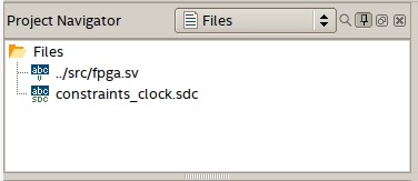
The sdc file contains the clock constraints.
 .
.This will all the necessary steps (synthesis, map, place & route, bit stream generation). This will also trigger a timing analysis to verify that the timing constraints are respected.
Make sure that the board is connected to the power supply and the power switch is ON. The USB programming cable must also be connected to your PC/workstation.

This should open the following window:
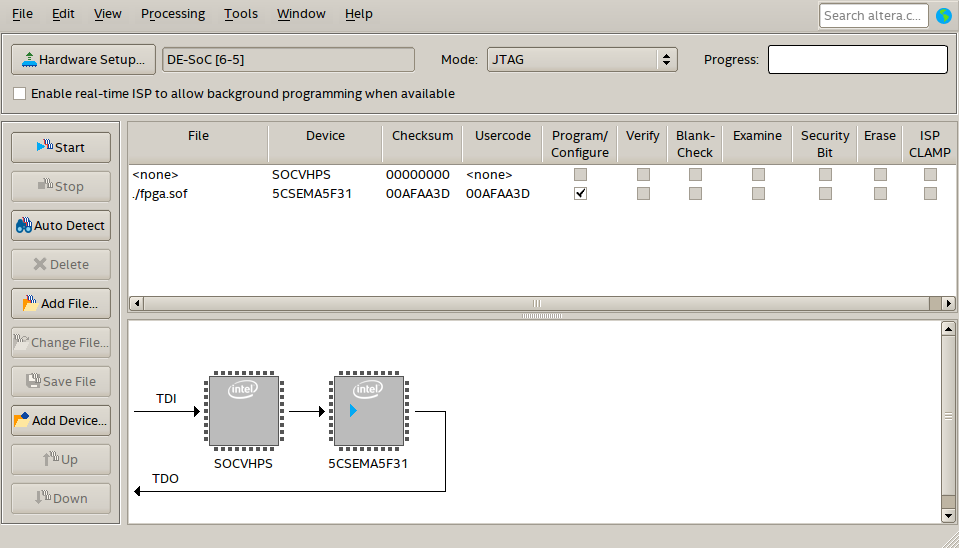
Clicking on the start button should program the FPGA.
| © Copyright 2022-2026, Tarik Graba, Télécom Paris. | |

|
Le contenu de cette page est mis à disposition selon les termes de la licence Creative Commons Attribution - Partage dans les Mêmes Conditions 4.0 International. |
| The content of this page is licensed under a Creative Commons Attribution-ShareAlike 4.0 International Licence. | |