
October 2025
The figure below shows simple Avalon Write and Read transactions.
Write transactions:
write signal.waitrequest signal.write signal is high and the waitrequest is
low.Read transactions:
read signal.waitrequest signal.read signal is high and the waitrequest is
low.In a simple Avalon implementation, Write and Read transaction can not be issued at the same moment.
One of the advantages of the Avalon protocol is that the implementation of simple memory mapped registers is straightforward.
The following figure represents a valid Avalon target(Agent).

As the waitrequest and read signals are
optionals, we can simply implement a compliant Avalon target by simply
describing a register with an Enable input.
writedata connected to the input of the registerwrite connected to the input of the enable
(EN in the figure) of the registerreaddata connected to the output of the registerAs a simple register can be updated in a single clock cycle when the
EN signal is high and its output is always valid at its
output, the waitrequest signal can be omitted (always low).
The read signal can also be omitted.
When integrating such a simple register using Platform Designer, the missing signals will be automatically added in the interconnect so the Initiator will have the correct signaling.
We will write a simple register that we will connect to the LEDs on the board. This module will replace one of the Altera/Intel PIO module.
Create a SystemVerilog file named simple_mm_register.sv.
The name is not really important, but generally, we use the same name
for the file and the module that it contains.
Remember, Verilog is case-sensitive
The module interface will contain the following signals:
clk : the main clockreset_n : an asynchronous, active low, reset
signalavs_write : the Avalon write
signalavs_writedata : the Avalon 32-bit
writedata signalavs_readdata : the Avalon 32-bit
readdata signalleds : 10-bit output to connect the 10 lower
bits of the register to the LEDs on the boardmodule simple_mm_register(
input clk,
input reset_n,
input avs_write,
input [31:0] avs_writedata,
output [31:0] avs_readdata,
output [9:0] leds
);
// the behavioural code will be added here
endmoduleA 32-bit register, with a reset value of 0. Its value is set from the
writedata input when the write signal is
high.
logic[31:0] R;

always_ff@(posedge clk or negedge reset_n)
  if(!reset_n)
    R <= '0;
  else if(avs_write)
R <= avs_writedata;We will use concurent assignments to connect the output of the
register to the readdata. Thus, we can read the content of
the register from the host (the Processor).
We will also connect the lower 10 bits of the register to the
leds output to have a visual feedback when testing on the
FPGA board.
assign avs_readdata = R;
assign leds = R[9:0];In the IP Catalog pane, click on new component. A wizard
will help un generate the necessary files to integrate the register to
our previously designed platform.
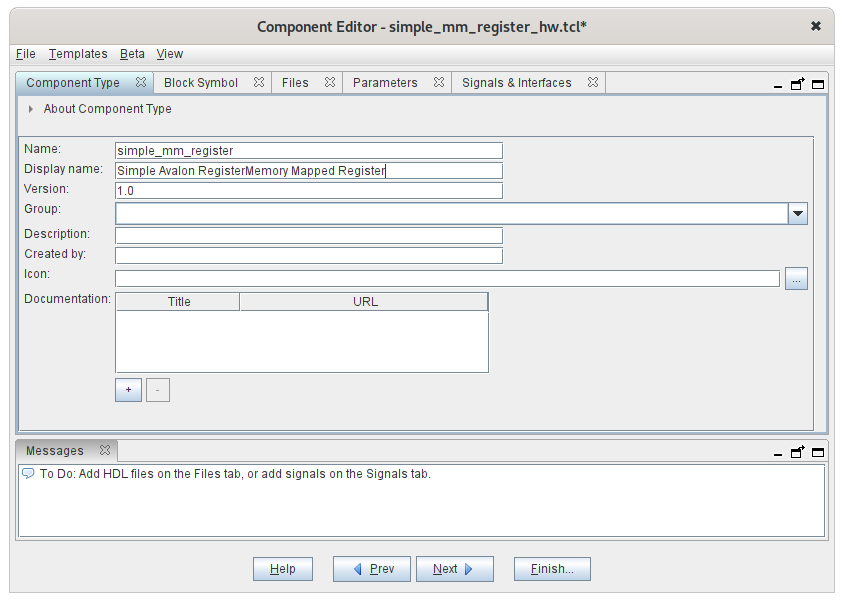
The first step is to choose a name and a display name. The name must not contain spaces or special characters.
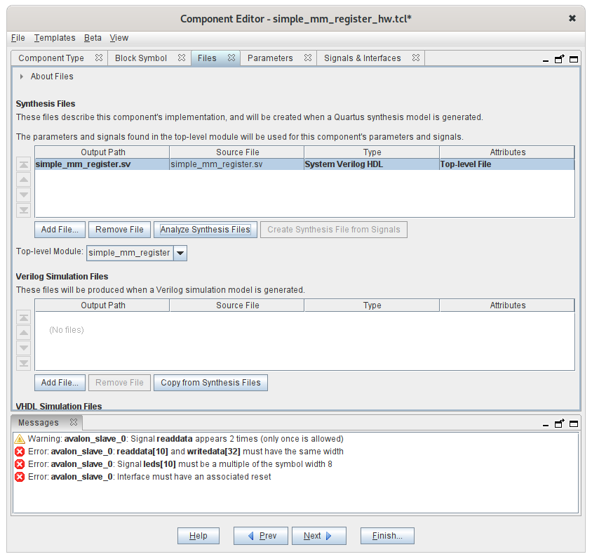
The second step is to add the RTL (Verilog here) files. By clicking
the Analyse Synthesis Files the tool will try to guess the
protocol that the design uses (Platform Designer supports other OnChip
protocols like AXI for exemple) and to map the module inputs/outputs to
the protocol signals.
After ths step some errors will appear, because the leds
output is also detected as a readdata output. We will
correct those errors in the next steps.
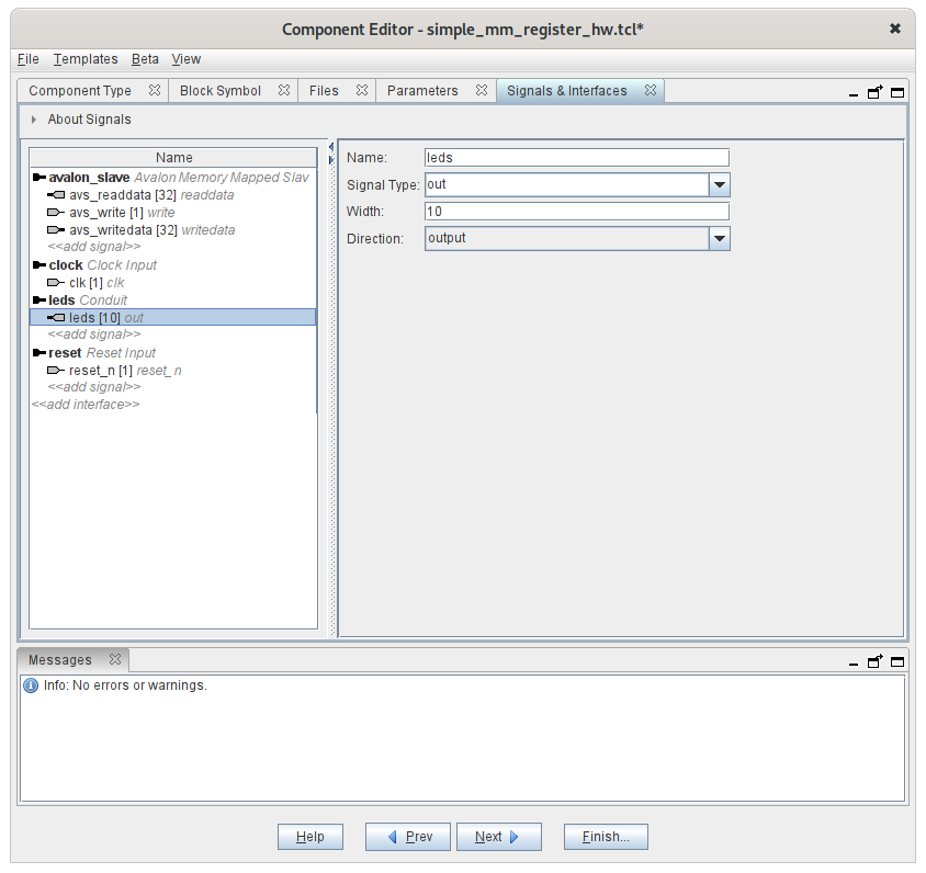
You can then go directly to the Signals & Interface
tab. Remove the leds signal from the
avalon_slave interface and add a conduit
interface. Add the leds 10-bit output signal to this
conduit as shown below.
The name of the signal must be the name of the output signal in the RTL design
Once completed, click on Finish. The new component
should appear in the IP Catalog pane.
Note
The component creation wizard will generate a
xxxx_hw.tcl script in the project directory. This file
contains the description of the module, the list of RTL files and the
description of the interfaces. The script is written in TCL and the
commands are documented in Platform
Designer documentation, so, these files can be written
independently, without using the wizard. Platform Designer will look for
_hw.tcl files in the project directory and in other
research path that can be modified in the tools preferences.
Remove the PIO module connected to the LEDs and replace
it by the new component that you have created. The updated design should
look as follows.
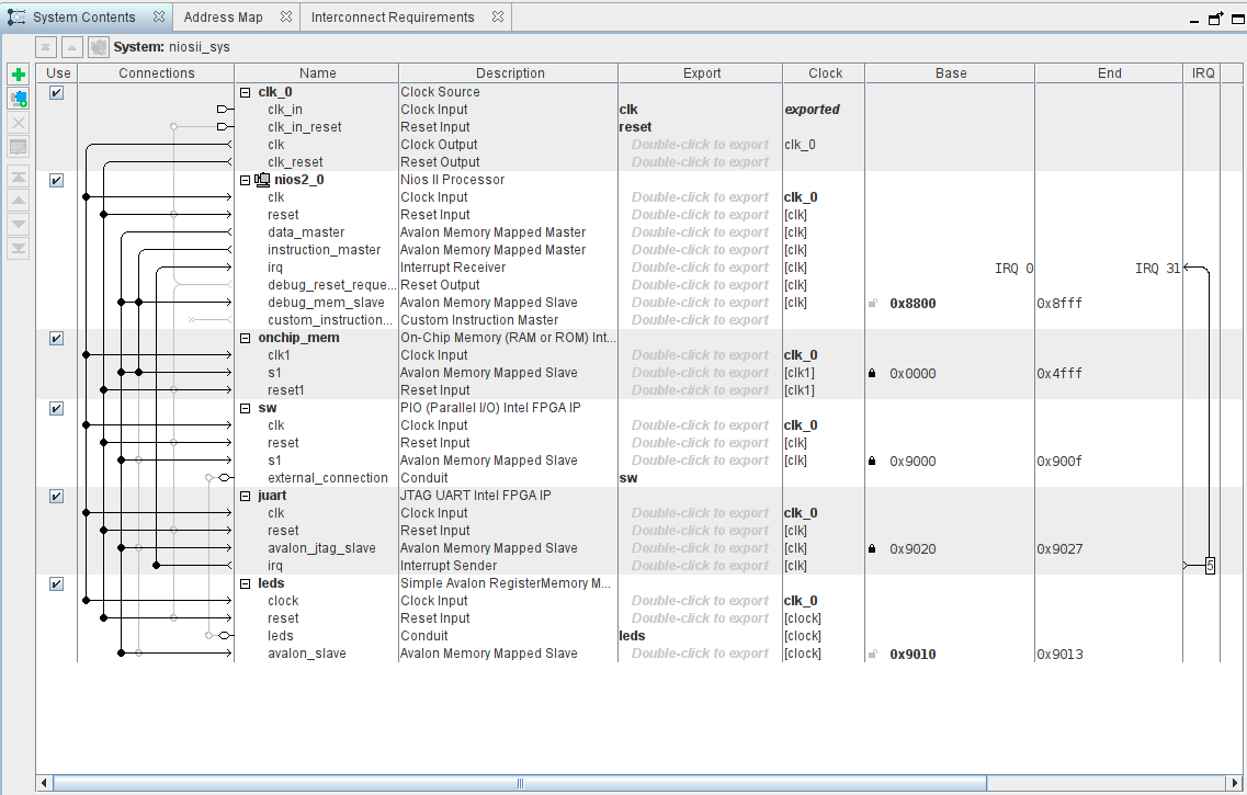
Once done (do not forget to reassign correct base addresses), you can save, generate the RTL and resynthesise the design in Quartus II. You should be able to reuse the test program from the first Lab to test your module.