
October 2025
The goal of this tutorial is to present Platform Designer as an example of tools to design a Processor System.
Platform Designer allows the integration of Intellectual Property (IP) hardware blocs around a Soft Core Processor (Nios II) or a Hard System (ARM HPS) through a graphical user interface. The tool allows automatic generation of interconnect logic without the need to write specific RTL (Verilog or VHDL) code.

In this tutorial we will go through the different steps to build a system around a Nios II soft processor core, and we will produce simple C code to interact with the different elements of the system.
The System that we will design is depicted in the following figure:
It is composed of the following elements:
BRAM)printf)The following steps will be carried out:
To simplify the integration in the FPGA synthesis flow, we will use a pre-build project. The project includes information about:
The base project archive can be downloaded here.
After downloading and decompressing the archive, you can open the project in the Quartus II software.
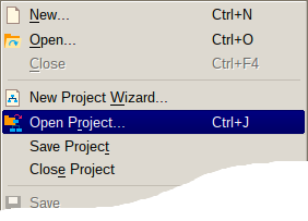
Open the provided project by selecting the
Open Project... item of the File menu and
locating the DE1-SoC.qpf project file.
This project contains a unique RTL (DE1-SoC.sv) file
with the Inputs/Outputs definitions. Some outputs have been assigned to
constant values (for example, the LEDs are turned off). This module
(DE1-SoC) is the top level block of our design and will
contain later the SoC system that we will design in Platform
Designer.
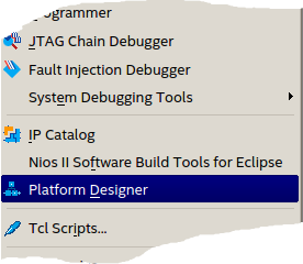
From the Tools menu, you can launch
Platform Designer.
This will create an empty integration project and should look as follows.
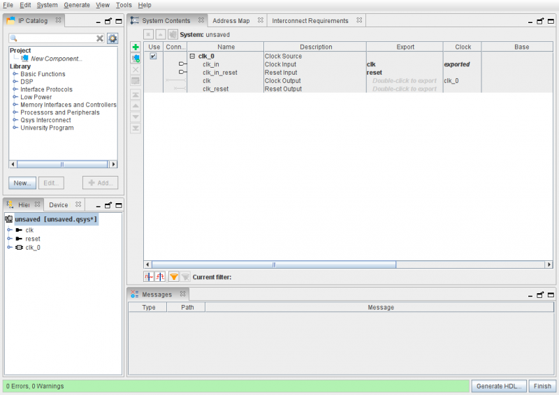
This is the starting point to construct our system.
The newly created system contains a clock and Reset submodule. Note
that in the Export column we have two signals (clk
andreset) that are exported which means that we will be
able to connect them to the clock and reset source in the RTL top
design.
The left lateral pane of the Platform Designer window should contain
an IP Catalog tab. This represents the Library of IPs that
are available and hat we can use in our design. The different blocks are
organized in browsable categories and a search field helps to find
specific blocs.
The first element that we will add is the Nios II
processor. You can find it in the
Processors and Peripheral/Embedded Processors section.
It can be added by double-clicking on the item name in the
IP Catalog pane. A configuration interface is presented
which allows the selection of the Core and its configuration.
For this tutorial, we will use the resource optimized
Nios II/e core.
By clicking the finish button, the core is added to the design.
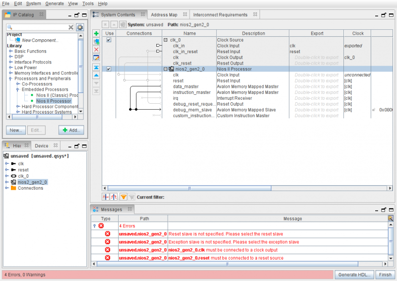
Some error messages are displayed because, for the moment, the processor is the sole element in our design, and it is not connected to any other element.
The second element that we will integrate in the design is an On-Chip
Memory. It can be found in the Basic Function.
This IP will use the FPGA embedded memory block and as they can be initialized with the FPGA bitstream, it can act as both Read Only Memory (ROM) for the program and constants and Random Access Memory (RAM) for data and variable.
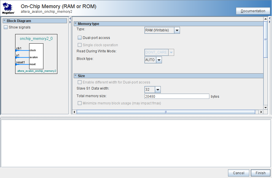
Change the Total Memory Size configuration to 20 KB as shown in the
following figure. This will allow using a simple C library with the
printf function.
Then we add two General Purpose Input/Output controllers (search for
Parallel I/O (PIO)). The PIO IP can be configured in width
and direction.
The first one will be used to attach to the 10 LEDs
(ledr output in the RTL top).
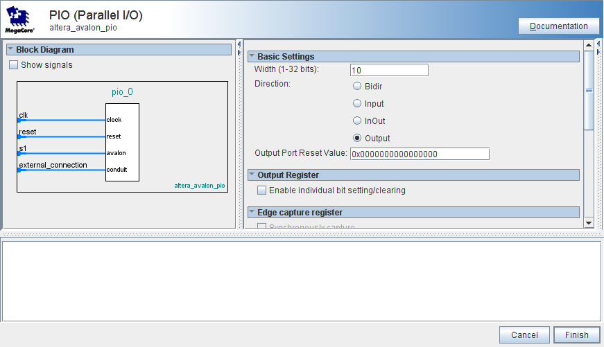
Modify the configuration of the PIO IP to have 10 outputs pins as depicted here.
The second PIO will be connected to the 10 switches (sw
signal in the RTL top). Thus, add a second PIO bloc with 10 pins
configured as inputs.
This last element can be found in Serial subsection of
Interface Protocols section. Keep the default configuration
this time.
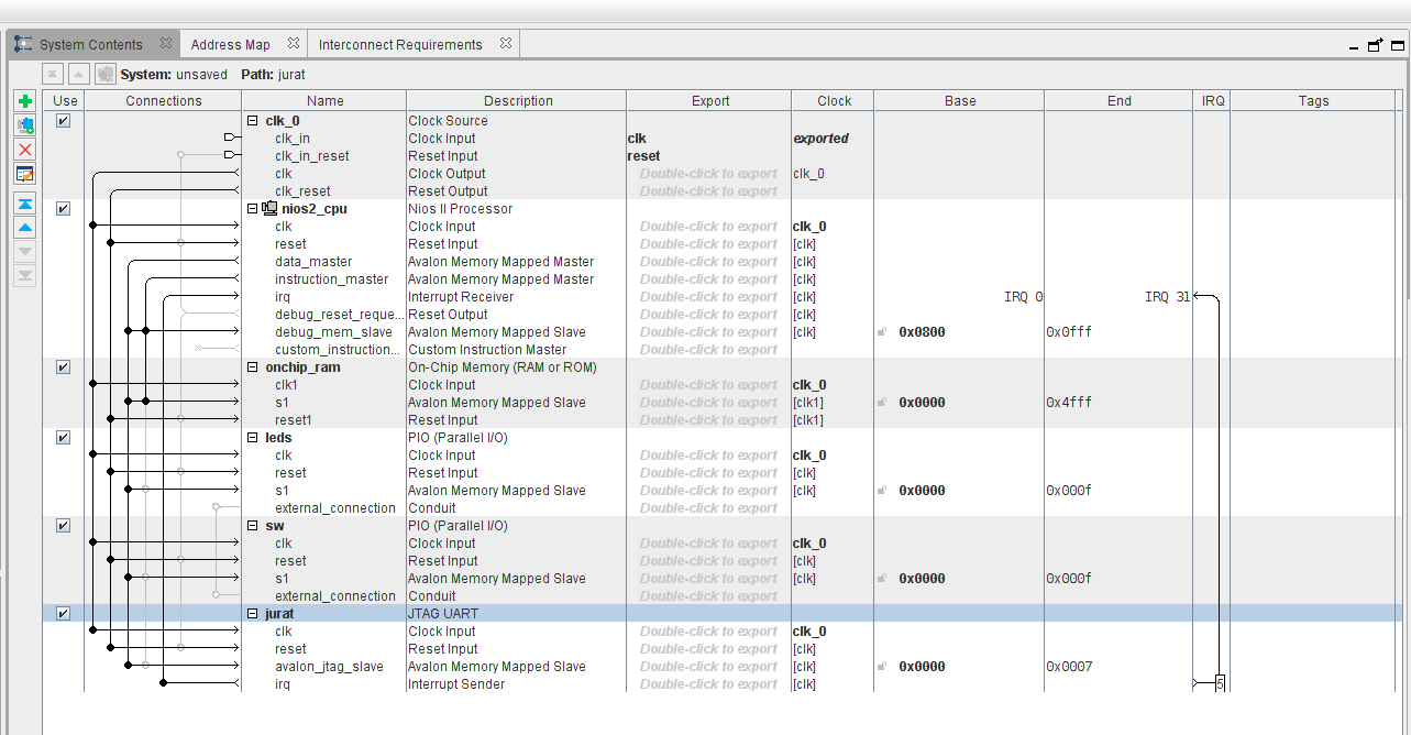
The connection’s matrix is visible in the Connections
column of the main window. The white dots represent possible
connections. When clicked, they turn black to signify that the
connection is effective.
The tool does not allow connections between incompatible interfaces (you can not connect an output clock to a reset input for example).
Here are the connections that we want to have in our system:
irq (interrupt request) output from the
jtag uart to the processor interrupt receiver.All connections done, the connection’s matrix should look as follows.
Remarks
CTRL-RIRQ column (here we have chosen to connect the jtag uart
irq to the irq number 5 of the processor).The column BASE show the base address of each
peripheral. For the moment, all peripherals have a base address equal to
0.
We can assign the base addresses manually, but we must take care of avoiding overlapping ranges.
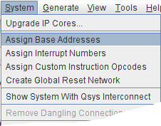
The tool provides a way to assign those addresses automatically
through the item Assign Base Adresses of the
System menu.
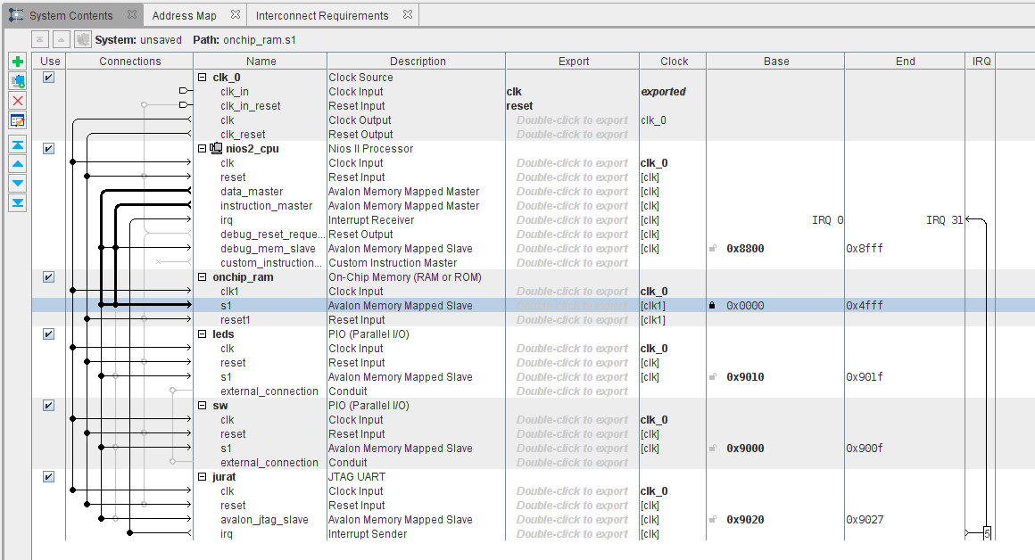
We want to keep the base address of the On-chip Memory at the value
0 even with the automatic assignation of base addresses. We
can lock this parameter by setting the lock symbol in the corresponding
line of the Base column. Then we can reassign base addresses
automatically.
The final address mapping should look like the following (some differences can exist depending on the order of appearance of the different IPs).
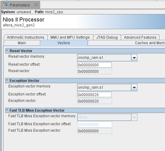
Now that the different addresses of the peripherals are set, we can go back to the processor configuration and set the reset and exception vectors. Those addresses correspond, respectively, to the address of the first instruction executed after a reset (or at the boot), and the address of the exception/interrupt handler.
By double-clicking on the processor in the main window, the
configuration pane should appear. In the Verctors tab you
can specify the reset and exception addresses, either by giving the
absolute value or by selection the peripheral name.
Here, we choose the On-Chip Memory instead of giving an absolute value, as it allows to change the mapping and size of the memory without loosing track
Normally, at this step, you should not have any error or warning message.
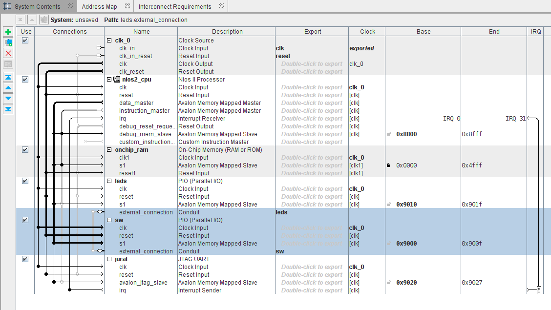
The inputs and outputs from the two GPIO controllers needs to be connected to the corresponding pins of the FPGA. To achieve this, the signals must be exported from the system to be connected in the top level RTL module.
In the main pane, for each PIO, you can export the external
connection, by double-clicking in the export column. There, you can
choose a explicit name, for example, here leds and
sw as it is shown in the following figure.
The last step, before going back to Quartus and synthesising the design, is to generate RTL files for the current project.
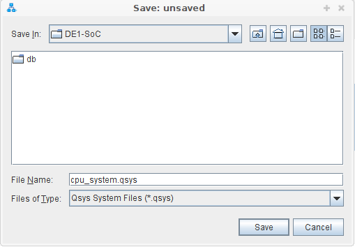
The first thing to do, is saving the project by choosing the
Save item in the File menu. Here you can
choose a explicit name for the system you have build (for example
cpu_system).
To generate the RTL, choose the Generate HDL from the
Generate menu.
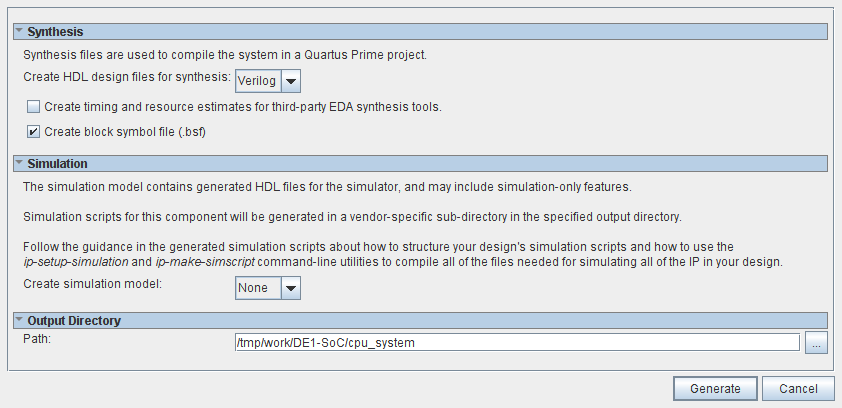
A directory with the same name as your system will be created in the Quartus project directory. Take some time to analyse the content of this directory.
You can now quit Platform Designer. A message will give you instructions on how to add the design to the Quartus Project. Ignore those instructions
In Quartus, select the Add/Remove files in project...
from the Project menu. Open the file chooser by clicking on
the ... icon and choose the .qsys file
corresponding to your system.
Once done, you must modify the top level Verilog file by adding an
instance of the system. A _inst.v file
(cpu_system_inst.v) should have also been created with an
example of how to instantiate your design.
We will use the clock_50 input as the main clock of our
system and the key[0] as reset signal. We will also connect
the exported signals from the PIO to the corresponding switches and leds
signals.
Here is en example of the instantiation:
//////////////////////////////////////////////////////////////////////
// Nios-II System
//////////////////////////////////////////////////////////////////////

    cpu_system u0 (
        .clk_clk       ( clock_50 ) ,
        .reset_reset_n ( key[0]   ) ,
        .sw_export     ( sw       ) ,
        .leds_export   ( ledr     )
    );
Note
ledr output is already assigned to a constant,
you must remove (or comment) this assignment.Once the instance is added, you can compile the design in Quartus. This will run the synthesis and generate the bitstream to program the FPGA.
Altera/Intel provides a software toolchain for the Nios-II processor. It is based on the GNU toolchain (gcc, binutils,…).
They also provide the Monitor Program, a simple interface to build, load and debug a software project.
Note
Here is a simple program to test the LEDs and Switches. It continuously reads the state of the Switches and writes them to the LEDs.
// define macros to access to the data registers of
// the LEDs and SWs PIOs
#define LEDS  (*(volatile unsigned int*) 0x00009010)
#define SW    (*(volatile unsigned int*) 0x00009000)

int main()
{
  while(1)
    LEDS = SW;

}
Note
To launch the Monitor Program, use the
intel-fpga-monitor-program in a terminal. The main window
is shown in the following figure.
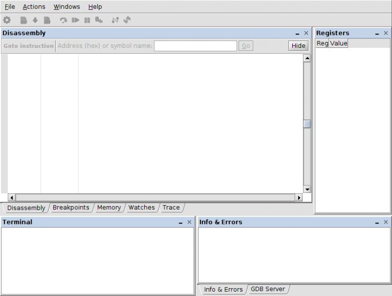
Let’s start with creating a new project from the File
menu and follow the assistant.
Choose a name and directory where the generated files will be created and select Nios II as the Architecture.
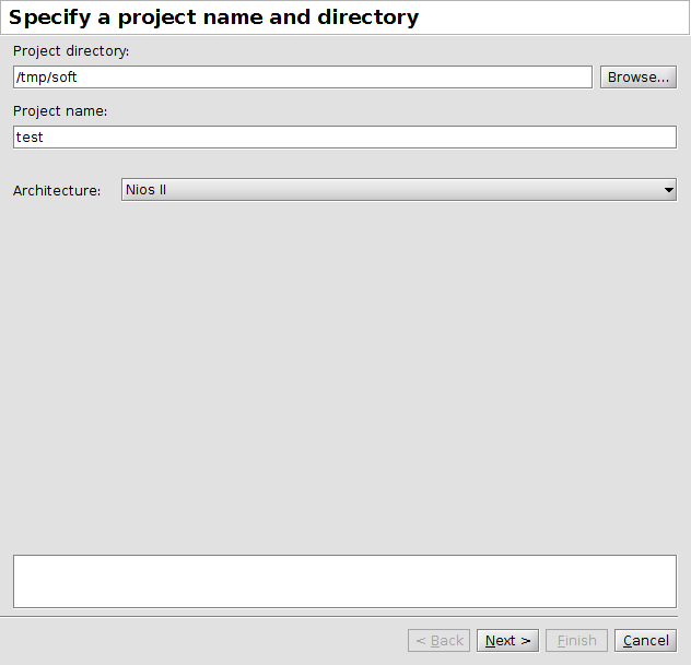
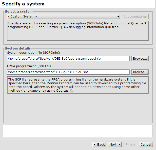
After clicking on the next button, you will be asked to specify the
target system. Here, you will have to select that you are using a
Custom System (the one that you have designed). And then,
select the System Description file .sopcinfo (that have
been generated by Platform Designer) and the FPGA programming file
.sof (the bitstream generated by Quartus) as shown in the
following figure.
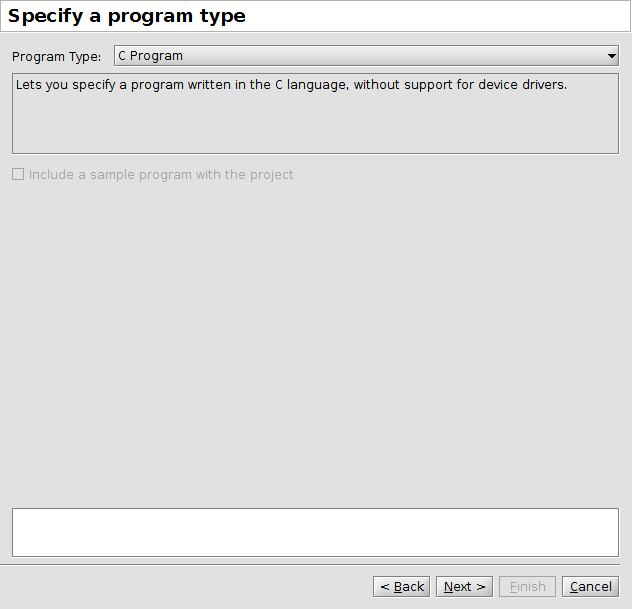
In the following pane, we will select C program type.
And then add the test C program.
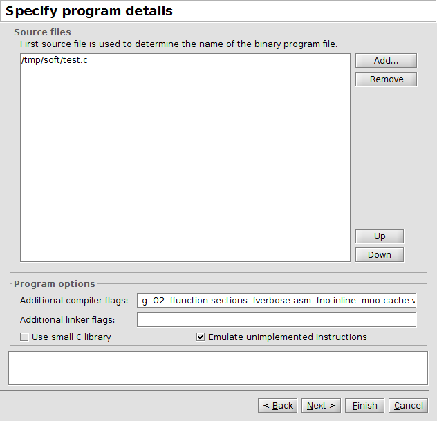
Her, you can also choose the software compilation options and
eventually add a small C library to your program (if you want to add
calls to printf for example).
The following steps, will ask you if you want to modify the memory organisation of your project. Just keep the default values and finish the configuration.
At the end, you will be asked to configure the FPGA and connect to the target system.
Note
Actions menu.Once connected to the target system, the main window will give you access to a simple interface to debug and run the software code.
Starting here, you can modify the C program, rebuild it and re-upload it. You can run the program continuously or step by step.